
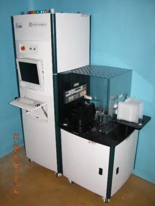
Description
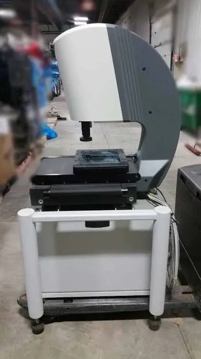
Year: 2004 Condition: Used Wafer Size: 200 mm Location: Ireland Equipment Details Equipment Type: High-Speed Wafer Inspection System Application: Bare Wafer Inspection Category: Semiconductor Metrology / Inspection Subcategory: Metrology Key Features 200 mm Wafer Capability High-Speed Wafer Inspection Bare Wafer Surface Inspection Automated Defect Detection Particle and Surface Defect Inspection Semiconductor Process Monitoring Description This 2004 high-speed wafer inspection system is designed for automated inspection of 200 mm bare semiconductor wafers. The system is intended for detecting particles, surface defects, and other wafer abnormalities during semiconductor manufacturing and quality-control processes. It is suitable for bare wafer inspection, incoming wafer quality control, process monitoring, semiconductor manufacturing, and research applications. Detailed model information, detection sensitivity, throughput, laser configuration, wafer handling configuration, software version, and current operational condition should be confirmed with the seller. For this 200 mm inspection system
Specifications
- Manufacturer
- AMAT
- Category
- Semiconductor & Electronics
- Condition
- USED
- Location
- Ireland
- Listed
- 1 month ago
- Views
- 146
Applied Materials Excite IPM 832
Ask price
oll309688
Identity revealed after deal is confirmed
Contact Seller
Related Products
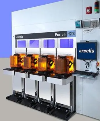
Axcelis PURION H200
Ask price
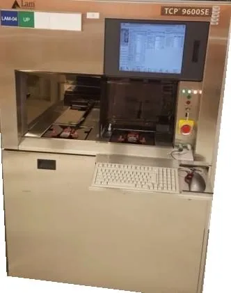
LAM TCP 9600SE
Ask price
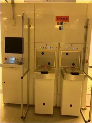
Rudolph S3000-S
Ask price
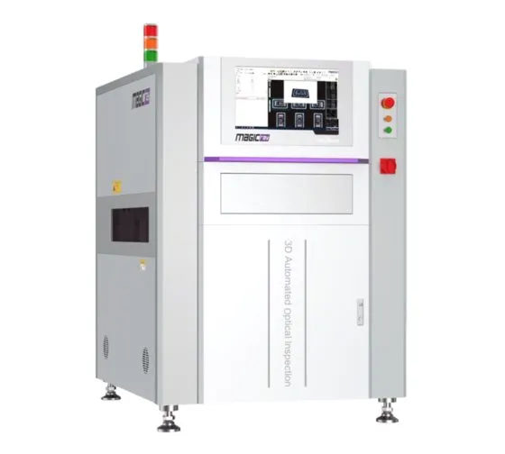
Cube-VS7000
Ask price
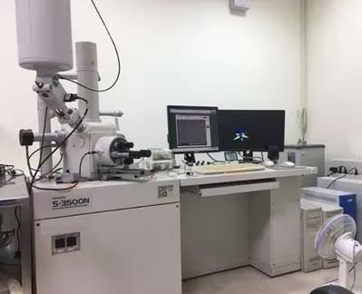
Hitachi Scanning Electron Microscope (SEM) S-3500N
Ask price
SEMVision CX+
Ask price
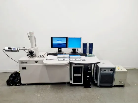
Hitachi S-2600N Scanning Electron Microscope + Oxford X-Max 50 mm2 Inca detector
Ask price
HEXAGON METROLOGY Optiv Performance 222
Ask price