
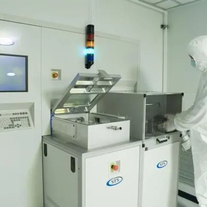
Description
Manufacturer: Applied Materials (AMAT) Model: SEMVision G2 Year: 2005 Condition: Used Wafer Size: 200 mm Location: Ireland Equipment Details Equipment Type: SEM Defect Review Station Configuration: Module Only Application: Semiconductor Wafer Defect Review Category: Semiconductor Metrology / Inspection Subcategory: Front-End Semiconductor Equipment Key Features SEM-Based Defect Review 200 mm Wafer Capability High-Resolution Defect Imaging Wafer Defect Analysis Semiconductor Process Monitoring Failure and Yield Analysis Description The Applied Materials SEMVision G2 is an SEM-based defect review system designed for detailed inspection and analysis of defects detected on semiconductor wafers. This unit is configured for 200 mm wafers and is intended for semiconductor defect review, process monitoring, failure analysis, and yield-improvement applications. The equipment is offered as a module only. Buyers should confirm exactly which components, electronics, computer, software, wafer-handling hardware, vacuum equipment, and accessories are included before purchase.
Specifications
- Manufacturer
- AMAT
- Category
- Metrology & Inspection
- Condition
- USED
- Listed
- 1 month ago
- Views
- 11
APPLIED MATERIALS SEMVision G2 Defect Review Station Module Only
Ask price
sal666050
Identity revealed after deal is confirmed
Contact Seller
Related Products
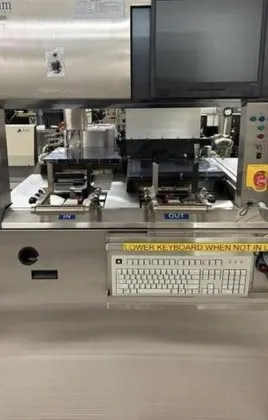
Lam 4520XLE
$84,000
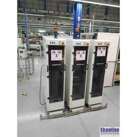
Europlacer Tray Sequencer
Ask price
XYZTec Condor 100 100-3
Ask price
Electro Design MB 706
Ask price
Electro Design MB 750
Ask price
Lam Research TCP 9600 SE Etcher
Ask price
KLA Tencor MicroXAM2 Interferometer System with Interface Box, Lamp PSU
Ask price
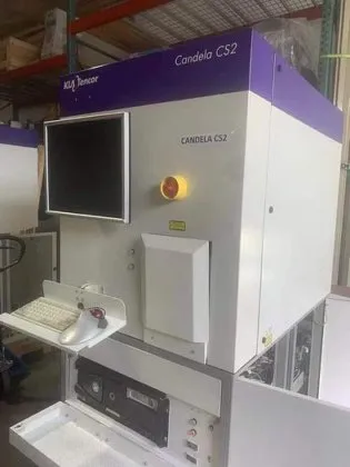
Particle Tester KLA-Tencor CANDELA CS2
Ask price