
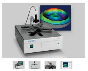
Description
The TMS-2000 can measure the flatness of the wafer with up to 1 nm repeatability. Conventional wafer thickness mapping techniques struggle with accuracy issues when used in unstable environments involving extreme temperature changes and vibrations while the TMS-2000 has high environmental stability. Thanks to its high-speed measurement capability and compact size, the TMS-2000 can be used in various industrial fields involving in-line inspection. ▪ High accuracy measurement using interferometric detection technique ▪Evaluation of flatness parameters in accordance with the SEMI standards ▪High environmental resistance ▪Compact device size for multiple applications ▪Spiral scanning (high speed, high density) (1 nm repeatability) Analysis Software The TMS-2000 comes with unique data acquisition software for consistent measurement, analysis and data output. The stage can hold up to 12 inch wafers, and once set, it automatically detects the notch position and wafer center effectively auto-loading coordinate data. In addition to thickness mapping and line profile analysis, flatness parameters compliant with SEMI standards can be statistically analyzed and the data can be output in any format. It can also analyze the thickness difference between the two specified wafers so it can be used for monitoring the polishing process.
Specifications
- Category
- Metrology & Inspection
- Condition
- USED
- Listed
- 1 month ago
- Views
- 21
TMS-2000, Wafer Thickness Mapping System
Ask price
fsm156258
Identity revealed after deal is confirmed
Contact Seller
Related Products
Lam 4520XLE
$84,000
Europlacer Tray Sequencer
Ask price
XYZTec Condor 100 100-3
Ask price
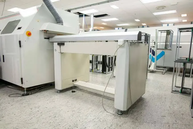
Electro Design MB 706
Ask price
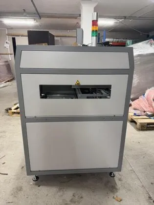
Electro Design MB 750
Ask price
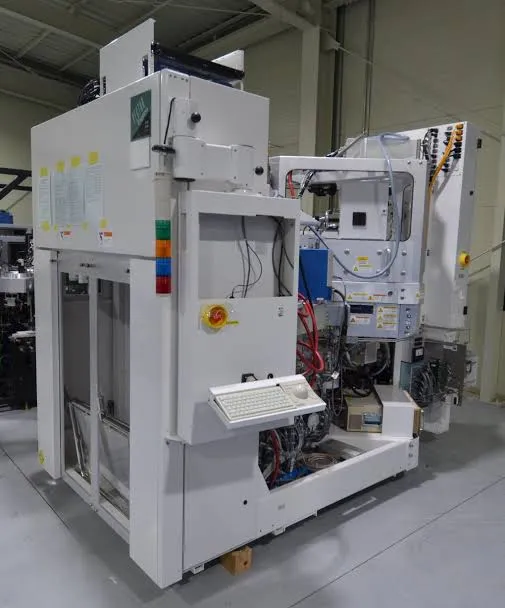
Lam Research TCP 9600 SE Etcher
Ask price
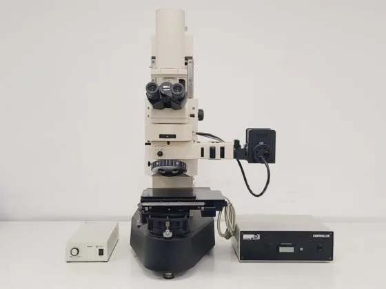
KLA Tencor MicroXAM2 Interferometer System with Interface Box, Lamp PSU
Ask price
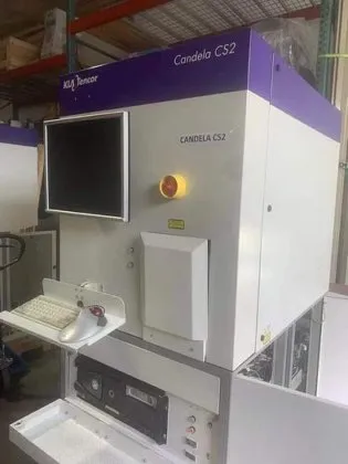
Particle Tester KLA-Tencor CANDELA CS2
Ask price