
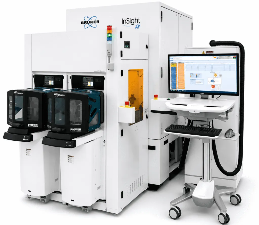
Description
Introduction The InSight AFP is Bruker’s fifth-generation automated atomic force profiler (AFP), offering the industry’s highest resolution, fastest profiling, and rapid 3D die mapping. It is positioned as the world’s highest-performance, industry-preferred CMP profiling and etch-depth metrology system for advanced technology nodes. Its modern tip scanner, combined with inherently stable capacitive gauges and an accurate air-bearing positioning system, enables non-destructive, direct measurement in the active area of dies — eliminating dependence on test keys or destructive cross-sectioning for many measurement tasks. Key Features TrueSense® technology delivering the proven long-scan capability of an atomic force profiler with the industry’s highest resolution and longest tip life Fully automated etch-depth, dishing, and erosion monitoring on submicron features with unsurpassed repeatability, without relying on test keys or models Proprietary CDMode for characterizing sidewall features and roughness, reducing the amount of required cross-sectioning and providing direct sidewall roughness data unobtainable through other techniques Automated defect review and classification, delivering fast, actionable topographical and material information on wafer and photomask defects for high-volume manufacturing (HVM) 100x high-resolution registration optics with AFM Global Alignment for less than ±250nm raw image placement accuracy on patterned wafers and masks 3D die mapping with HyperMap™, enabling full reticle-field scans with automated hot-spot detection and review Full compatibility with KLARITY and most other yield-management systems (YMS) InSight AFP Operating Principle The InSight AFP operates as an automated atomic force profiler: a tip-scanning head with capacitive position sensing and air-bearing stage positioning traces the surface topography of a sample in a closed-loop, force-feedback manner, generating direct, non-destructive 3D measurements within the active die area rather than relying on modeled or test-key proxies. Two proprietary adaptive modes extend this core principle: DTMode, an adaptive scan mode proven to deliver the lowest Total Measurement Uncertainty (TMU) of any AFM for depth metrology, and TrueSense™ mode, which relies on instantaneous feedback enabling picoNewton force control for the highest-accuracy, non-destructive surface profiling. After Polish Hot Spot Inspection - Scan Rate: 26 mm/sec; Number of scan lines: 33,000 Measurement Capabilities CMP post-polish residual topography detection with picometer sensitivity Etch depth, dishing, and erosion measurement on submicron features Sidewall feature and roughness characterization (CDMode) Top Line Roughness (LTR) measurement for EUV lithography process monitoring Resist profile shrinkage characterization for EUV process development Automated defect topography and classification review
Specifications
- Category
- Semiconductor & Electronics
- Condition
- NEW
- Listed
- 1 month ago
- Views
- 19
InSight AFP — Automated Atomic Force Profiler for Semiconductor Metrology
Ask price
fsm156258
Identity revealed after deal is confirmed
Contact Seller
Related Products
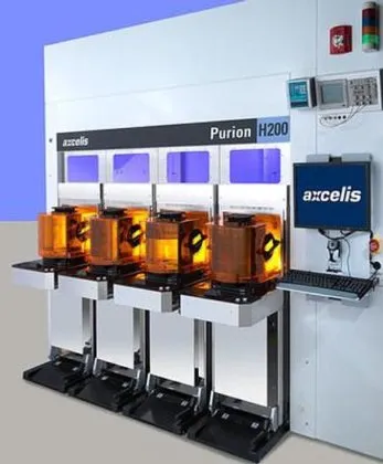
Axcelis PURION H200
Ask price
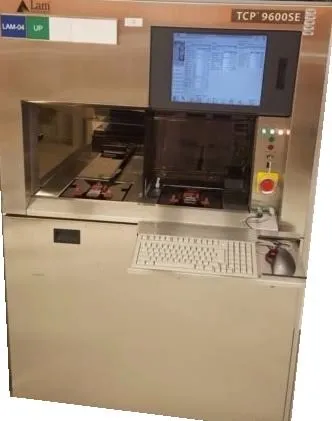
LAM TCP 9600SE
Ask price
Applied Materials Excite IPM 832
Ask price
Rudolph S3000-S
Ask price
Cube-VS7000
Ask price
Hitachi Scanning Electron Microscope (SEM) S-3500N
Ask price
SEMVision CX+
Ask price
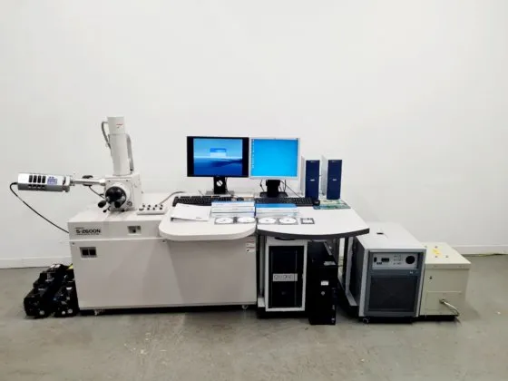
Hitachi S-2600N Scanning Electron Microscope + Oxford X-Max 50 mm2 Inca detector
Ask price