
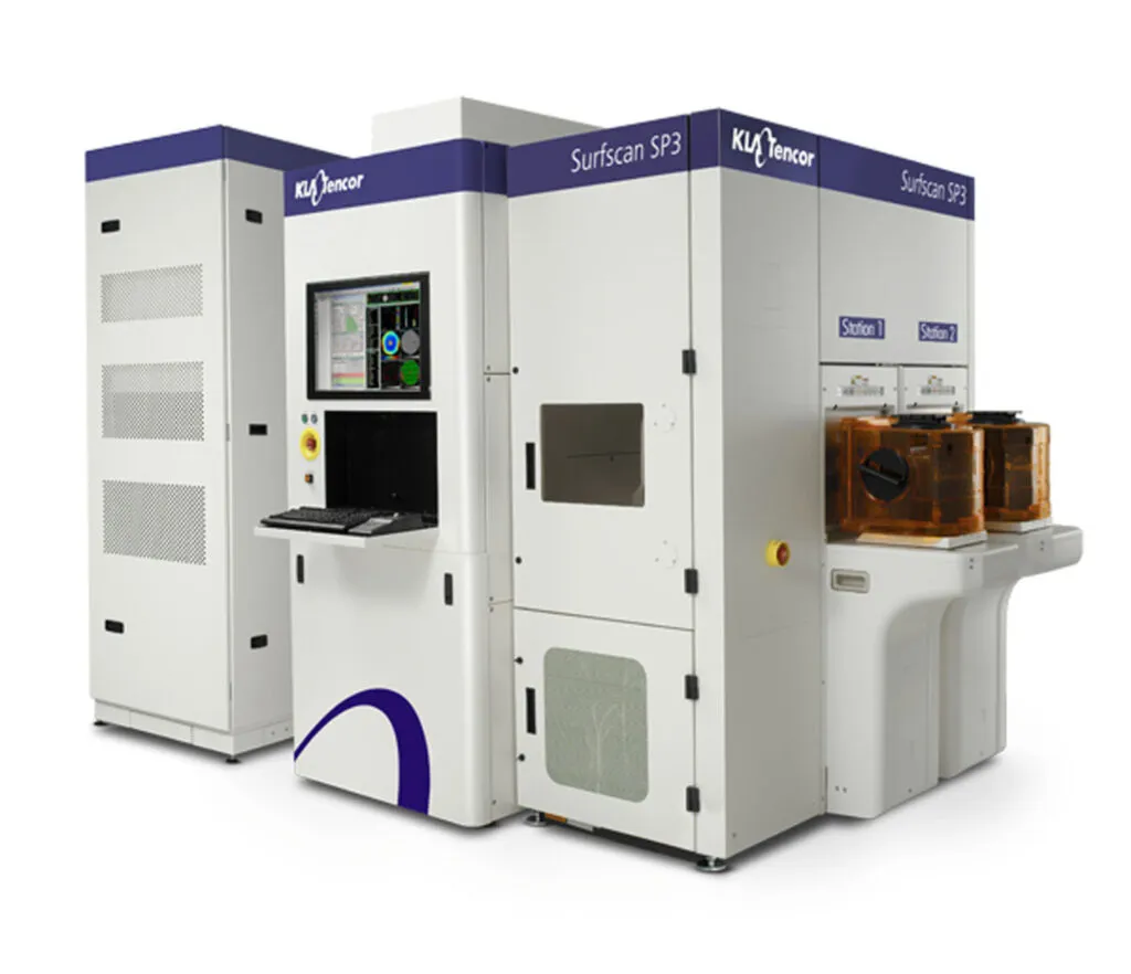
Description
Introduction The Surfscan SP3 is the first unpatterned wafer inspection platform to incorporate deep-ultraviolet (DUV) illumination, featuring dramatic advances in sensitivity and throughput over its predecessor the Surfscan SP2XP. It is designed for substrates targeting less than 28nm devices. Key Features DUV light source and DUV-optimized optics for capturing critical defects at advanced nodes (28nm and below) Sensitivity to sub-40nm defects, driven by the DUV source, DUV-optimized optics, and advanced detection algorithms Standard darkfield inspection with an optional brightfield channel; both modes can run concurrently for capturing and classifying a wide range of yield-critical and latent defect types in a single pass Optional brightfield channel specifically for detecting large substrate defects such as epi stacking faults and air pockets Automated defect signature detection and classification to speed identification and root-cause sourcing Integrated SURFmonitor capability for process optimization, surface roughness measurement, and capture of ultra-fine slip lines and scratches Optional backside inspection module for detecting defects that could deform wafer shape during photolithography Cross-model matching and correlation across the Surfscan SP1, SP2, SP3, SP A2, and SP A3 family Platform architecture designed with extensibility toward larger substrate formats (a dedicated Surfscan SP3 450 configuration was developed for 450mm wafers) Surfscan SP3 Inspection Capabilities Modes: Darkfield (standard) and brightfield (optional), operating concurrently Resolution: High-resolution (~100 megapixel) full-wafer SURFmonitor haze maps for automated capture of ultrafine slip lines, scratches, surface roughness, and grain size data Surface characterization: Surface quality characterization and surface roughness measurement integrated into the inspection workflow Process monitoring: Supports mapping of film thickness and roughness uniformity, and identification of annealing issues Detectable Defect Types Sub-40nm particle and pattern defects Epi stacking faults and air pockets (large substrate defects) Ultra-fine slip lines and scratches Surface roughness and haze anomalies Grain size variation Latent reliability-impacting defects Backside wafer defects affecting lithographic flatness Supported Wafer Sizes 150mm, 200mm, and 300mm, with a dedicated Surfscan SP3 450 configuration developed to support 450mm wafers for polished silicon and epitaxial silicon substrates.
Specifications
- Category
- Semiconductor & Electronics
- Condition
- USED
- Location
- Mipitas, CA, USA
- Listed
- 1 month ago
- Views
- 16
Surfscan SP3 Unpatterned Wafer Inspection Systems
Ask price
fsm156258
Identity revealed after deal is confirmed
Contact Seller
Related Products

Axcelis PURION H200
Ask price
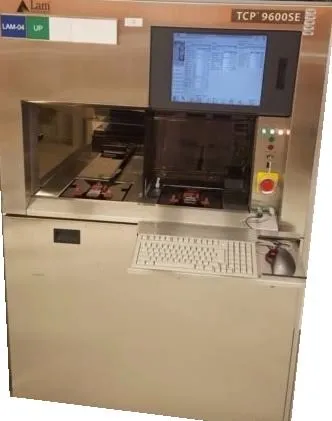
LAM TCP 9600SE
Ask price
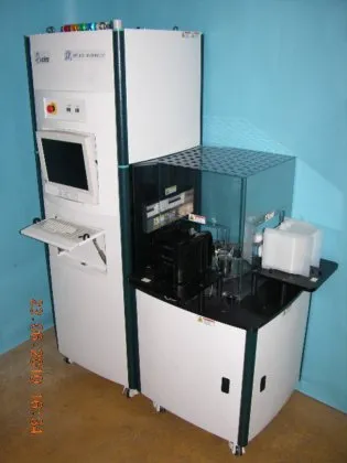
Applied Materials Excite IPM 832
Ask price
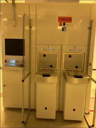
Rudolph S3000-S
Ask price

Cube-VS7000
Ask price
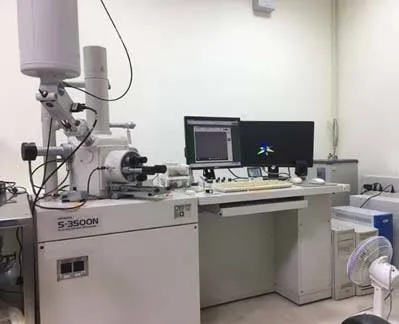
Hitachi Scanning Electron Microscope (SEM) S-3500N
Ask price
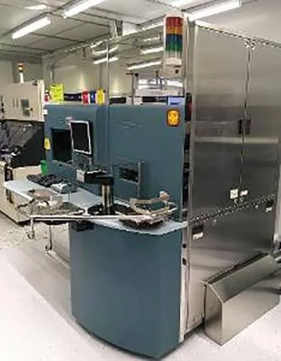
SEMVision CX+
Ask price
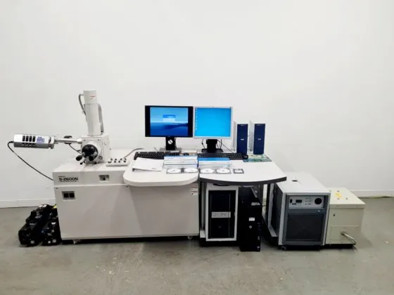
Hitachi S-2600N Scanning Electron Microscope + Oxford X-Max 50 mm2 Inca detector
Ask price